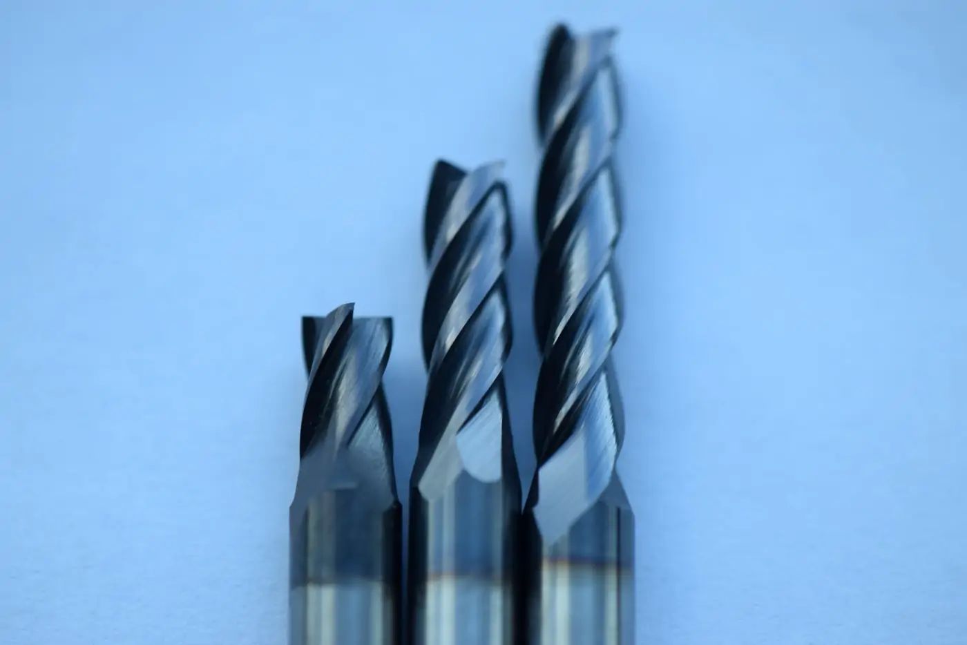
Surface treatment options for engineered components have expanded well beyond the legacy methods that dominated manufacturing for decades. Engineers and procurement teams evaluating coatings for wear resistance, friction reduction, or corrosion protection now choose between physical vapor deposition, CVD (Chemical Vapor Deposition), thermal spray, and electroplating. Each process produces a different type of surface, and the differences in thickness, adhesion, substrate impact, and environmental profile determine which one fits the application.
How Each Process Works
Physical vapor deposition coating is a vacuum-based process. A solid target material is vaporized through arcing or sputtering and deposited as a thin, hard film onto the part surface. The process operates at relatively low temperatures (typically below 500°C), and the resulting coatings range from 1 to 7 µm with hardness values from 1,800 to 4,500 HV.
CVD uses chemical reactions between gaseous precursors at higher temperatures (often 800 to 1,100°C) to deposit coatings onto the substrate. DLC (Diamond-Like Carbon) is one exception, applied through CVD at lower temperatures. CVD coatings provide excellent coverage on internal surfaces and complex geometries because the reactive gases reach all exposed areas, not just line-of-sight surfaces.
Thermal spray processes (plasma spray, HVOF, flame spray) melt or semi-melt coating material and propel it onto the part surface at high velocity. The resulting coatings are substantially thicker, typically 50 to 500 µm, and mechanically bonded rather than atomically bonded to the substrate.
Electroplating deposits metal (commonly chromium, nickel, zinc, or cadmium) from a liquid chemical bath onto the part surface using electric current. Hard chrome plating produces coatings at 5 to 250+ µm with hardness around 800 to 1,000 HV.
Thickness and Dimensional Impact
The most immediate practical difference between these processes is how much material they add to the part surface.
Physical vapor deposition coating at 1 to 7 µm adds minimal material to the part surface. A 3 µm coating adds 6 µm to the total diameter of a cylindrical component, which for many precision-machined parts falls within allowable tolerance bands. Post-coating grinding is not typically required, though dimensional impact should be verified against the specific tolerance requirements of each part.
CVD coatings are similarly thin (1 to 25 µm depending on type), though higher deposition temperatures can affect substrate properties. Thermal spray at 50 to 500 µm and electroplating at 5 to 250+ µm add substantially more material, which in many cases requires post-coating machining to restore dimensional accuracy. The additional step adds cost, lead time, and the risk of introducing surface defects.
Adhesion and Coating Integrity
Physical vapor deposition produces coatings that bond to the substrate through the vacuum deposition process, forming a dense, well-adhered film at the surface. When the substrate is properly cleaned and the coating-substrate pairing is compatible, PVD films are generally resistant to chipping, flaking, and delamination under typical operating loads and thermal cycling conditions.
CVD coatings also bond well, particularly on complex geometries. Thermal spray coatings rely on mechanical interlocking between the sprayed particles and the roughened substrate surface, which makes them more susceptible to spallation under impact or thermal shock. Electroplated layers bond through electrochemical deposition and may be more susceptible to peeling, blistering, or cracking under certain thermal cycling or mechanical stress conditions. Hydrogen embrittlement can also be a concern with chrome plating on high-strength steels and superalloys, depending on the substrate and plating process used.
Substrate Impact
PVD’s low processing temperature (typically below 500°C) generally preserves the substrate’s heat treatment, hardness, and mechanical properties. For most hardened tool steels and common substrates, the part exits the PVD chamber with its core properties intact, though compatibility should be confirmed for temperature-sensitive materials or specialized heat treatments.
CVD’s higher processing temperatures (800 to 1,100°C for standard CVD) can alter the heat treatment of the substrate, limiting its use on temperature-sensitive materials. Thermal spray generates localized heat at the surface but can induce residual stress in the substrate. Electroplating operates at low temperatures but introduces hydrogen into high-strength substrates, requiring post-plating baking to reduce embrittlement risk.
Environmental Profile
PVD is a dry vacuum process with no liquid chemical baths, no heavy metal discharge, and no hazardous wastewater. CVD uses gaseous precursors that may include hazardous compounds depending on the coating type, though the process is contained within a sealed reactor.
Thermal spray processes generate overspray, particulate waste, and noise, though they avoid liquid chemical waste. Electroplating, particularly hard chrome plating, uses hexavalent chromium (Cr6+), a known carcinogen. Regulatory frameworks including REACH (EU), RoHS, and EPA NESHAP standards increasingly restrict hex chrome use, driving manufacturers toward cleaner alternatives. For operations evaluating long-term regulatory compliance alongside surface performance, physical vapor deposition provides wear resistance, friction reduction, and corrosion protection, depending on the coating type selected, without the environmental and regulatory burden that accompanies electroplating.